
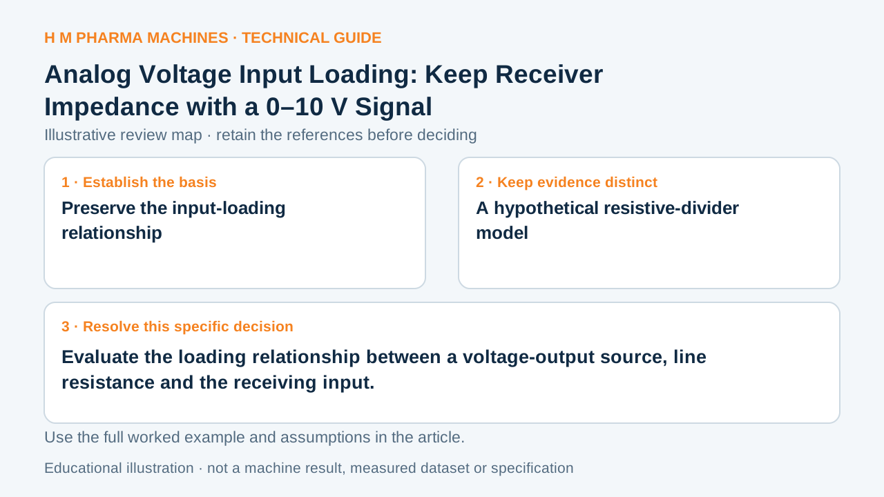
A voltage-output label does not establish that every receiving input leaves that voltage unchanged.
Preserve the input-loading relationship
TI's industrial analog-input reference uses a high-impedance buffer to avoid source-impedance interaction with its following stage. Preserve input impedance when reviewing a voltage interface. Primary reference: TI industrial input, section 2.1.
Define the source's equivalent output resistance, any modeled line resistance and the receiving input resistance. These belong to the analog signal path, not the separate power-supply distribution calculation. A nominal 0–10 V output span does not by itself describe loading by the selected receiver.
A hypothetical resistive-divider model
Assume an ideal 5 V source followed by a total series resistance of 1 kΩ and a receiver modeled as 9 kΩ. The receiver voltage is 5 × 9/(1 + 9) = 4.5 V. This simplified steady-state model has no reactive elements and treats the input as an ordinary resistance. Its result comes from the stated assumptions, not an installed sensor test.
Put the ideal voltage, combined series resistance, receiver resistance, calculated terminal voltage and omitted effects in separate worksheet cells. Do not copy the model into an active-output design without checking that the real component specifications justify those assumptions.
Ask for applicable interface evidence
The actual source may define output-drive limits and the receiver may specify impedance differently across conditions. Keep the relevant definitions and component revisions with the interface review rather than assuming infinite input resistance.
Record whether the proposal includes both ends of the signal path. If the receiver changes, revisit loading even when the stated voltage span is unchanged. This guide identifies a specific missing relationship; it provides no universal acceptable resistance ratio, cable-length promise, buffer design or HM output specification.
Customer Questions
Does a 0–10 V label prove the receiver sees the ideal source voltage?
No. Review the applicable source and input loading.
Is the 4.5 V result an HM measurement?
No. It follows a hypothetical resistive-divider model.
Can an active output always be modeled by one resistance?
No. The actual interface specifications must justify the model.
Primary References
These references support the technical principles discussed in this guide. The worked examples and review questions are educational.
Discuss Your Machine Requirement
Share your product, container, required output and the evidence needed for your technical review.
Request a Technical Review